UV LED for Electronics Application: Why it’s Critical
UV LED curing is the technique of curing adhesives, coatings, and encapsulants using the ultraviolet light emitted from LEDs. In the manufacturing of electronics, this technique is useful for instant photo degradation of materials without exposing a great deal of heat to components, which is a concern for delicate parts.
In comparison to generic mercury UV lamps, UV LED systems provide:
° Strictures for use during diagnosis or surgery.
° Environmentally friendly technology.
° Process temperature that does not damage components.
° Uniform temperature distribution via rapid cooling features.
° Curing methods that utilize barrier materials such as UV filters during the treatment stage.
° On/Off switching for enhanced energy savings.
Why it Critical in Electronics Manufacturing?
Enclosures for modern electronics usually have fine pitch, soft, and easily warped chips. Integrated circuits also combine a large number of highly miniaturized parts mounted on the surface. These components are highly sensitive to temperature, pressure, and other forms of mechanical or thermal stress. Conventional curing techniques using thermal ovens or mercury UV lamps achieve high rates of curing, but run the risk of overheating delicate chips, which can result in warping, damage, or even permanent failure. These problems are solved through low-temperature, precision curing using UV LED curing, thus ensuring that devices maintain their structural integrity and functioning.
Key Benefits:
• Provides miniaturization for devices with fine-detail representation.
• Greater automation for speed in mass production.
• More accurate, uniform precision, and reproducibility.
Highlights of the LED Curing Systems from UVET
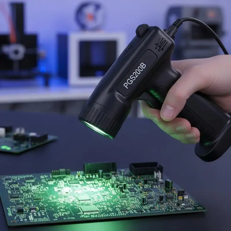
- Accurate Curing
Through UVET’s curing heads, the supply of focused UV energy allows for the exact curing of fine features or tight spots in microelectronics assemblies. Best for thin lines, intricate traces, and small surface areas.
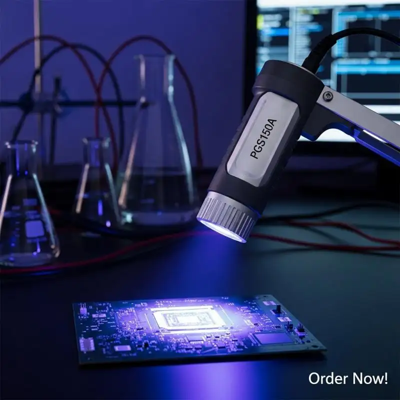
- Zero Thermal Damage
Our available systems are unique in comparison to traditional heat-based or mercury UV curing because they operate with minimal thermal output, which preserves and prevents damage to components.
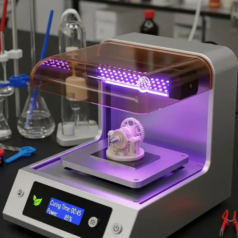
- Ready for Miniaturization
The ability to non-contact cure pinpoint with UV LED makes it suitable for advanced devices such as wearables, AR/VR gadgets, and IoT sensors, as components get smaller.
- Compact and Modular Design
Seamless integration is achieved with SMT pick-and-place, dispensing, and inspection systems because our compact UV LED modules can be placed into any automated line or robotic arm.
Applications: Industries Where UV LED Curing is Employed
UV LED curing is incorporated in various processes in the manufacturing of electronics. The following are the most common work types and their applications that are taught in various electronics and engineering schools.
1. PCB Solder Masking
Submersible solder masks that range from 0.2mm to 0.5 mm are placed on printed circuit boards (PCBs) to prevent corrosion, oxidation, and other forms of short circuiting. Each mask is done to a micron-level precision with UV LED curing, ensuring that the solder mask extends over the boundaries.
2. Display Lamination
Optical adhesives that are used in the construction of displays, LCDs, and OLEDs require strength, transparency, and responsiveness. They need to be bonded onto glass as well as flexible films while maintaining their shape. This is accomplished using Curing, which manages to bind without the bubble.
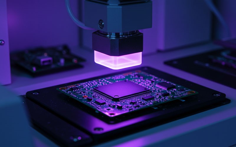
3. Chip Encapsulation
Microelectronic components, along with semiconductor chips, need to have their moisture résistance and mechanical support sealed. The use of curing in hardening encapsulate materials is achieved with precision, which helps in sealing the microchips as well as MEMS devices.
4. Module assembly
The advanced technology from smart mobile phones, along with drones and medical imaging devices, has led to compact camera module successors. Precise adhesion in sensors, along with lenses and housing units, is made possible by curing, therefore allowing better alignment and optical precision.
UVET is the best provider of UV LED curing for electronics
Delivering unrivaled service UVET specializes in curing applications for PCB solder masking, display lamination, and chip encapsulation with over a decade of experience in R&D on UV LED curing for electronics. Their systems are able to provide advanced solutions for precision, performance, and efficiency, ensuring no thermal damage is applied to components and maintaining micron-level accuracy for curing processes.
Applied UV LED Achievements:
Businesses across the electronics industry value chain are incorporating UVET’s UV LED curing systems to improve speed, reliability, and output. Below are examples of our technology:
• Over 40% reduction in display bonding defects was achieved by one of the global smartphone manufacturers using UVET’s 365nm LED curing system during the lamination step.
• A PCB fabricator used our high-power LED modules on its masking line and increased the throughput by 60%.
• A chip packaging plant uses UVET’s compact air-cooled curing heads to encapsulate microchips with sensitive silicon wafers safely without damaging the surfaces.
Save the environment with UV LED technology
UVET-based curing systems are effective UV LED devices and environmentally friendly, and some of the key features are:
• Save up to 70% in energy consumption when compared to mercury lamps.
• Long lifetime with minimal maintenance and parts replacement.
• Instant ON/OFF switching is ideal for automated high-speed production lines.
• No hazardous materials are used, thus complying with green manufacturing policies.
Tailored UV LED Solutions for ODM/OEM Electronics Manufacturing
UVET specializes in custom-designed applications of UV LED for different processes of electronic fabrication, such as:
• Curing adhesives on micro components, displays, and PCBs.
• UV-printing for product labels and electronic components.
• UV encapsulation of integrated circuits, sensors, and other miniaturized chips.
• Vital components of an electronic assembly require cleanroom-capable ultraviolet sterilization.
As an OEM or ODM, we provide full service from design and prototyping, through testing and production, positioning us as your sole partner for all your UV LED curing requirements.
Conclusion
UV LED curing technology is transforming the processes involved in assembling, encasing, and safeguarding electronic devices. It provides the precision, thermal treatment, and energy required for modern high-tech, compact devices, and is simply efficient.
Together with UCET's advanced technology and unparalleled market support, your manufacturing line is future-ready, offering unmatched reliability, cleaner operations, and minimized lead times for high-quality output.
Achieve the best results from UV LED curing in electronics manufacturing by partnering with UVET, and contact us to tackle your next ground-breaking idea.
Share on Social:


- PREV: Null
- NEXT: UV LED for Automotive: Advanced & Efficient Solutions