What is Semiconductor Tape Curing?
Semiconductor tape curing describes the management of the hardening of the adhesives and protective tapes in semiconductor processes. These tapes play an important role in such steps as:
- Wafer dicing - securing fragile wafers through dicing.
- Back grinding - providing stability in wafer thinning.
- Die attach- attaching semiconductor die to packages.
- Packaging - sealing, encapsulation, and lamination.
Tapes without proper curing lose their adhesion, add defects, and reduce yield. The strengthening of bonds, improvement of adhesion, and long-term reliability are secured through the curing process.
UV Tape Curing
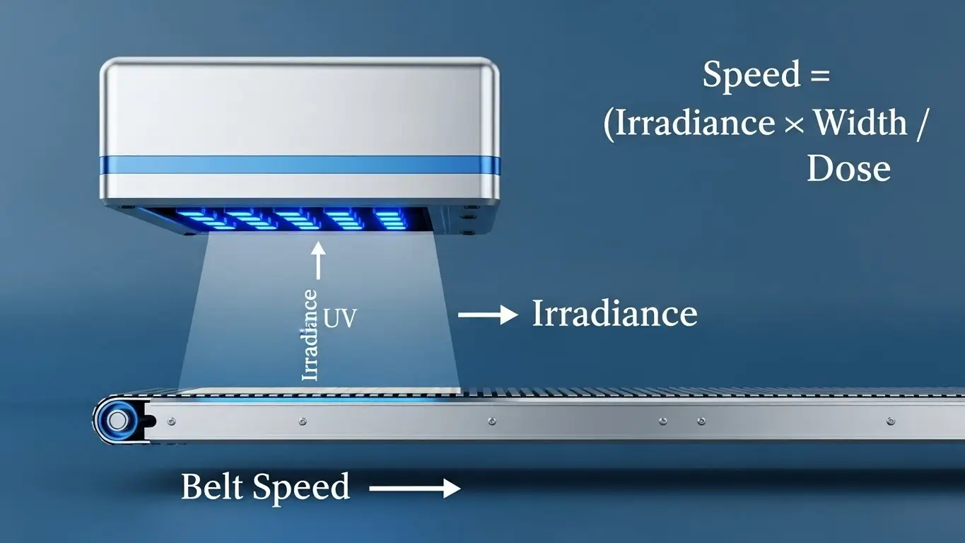
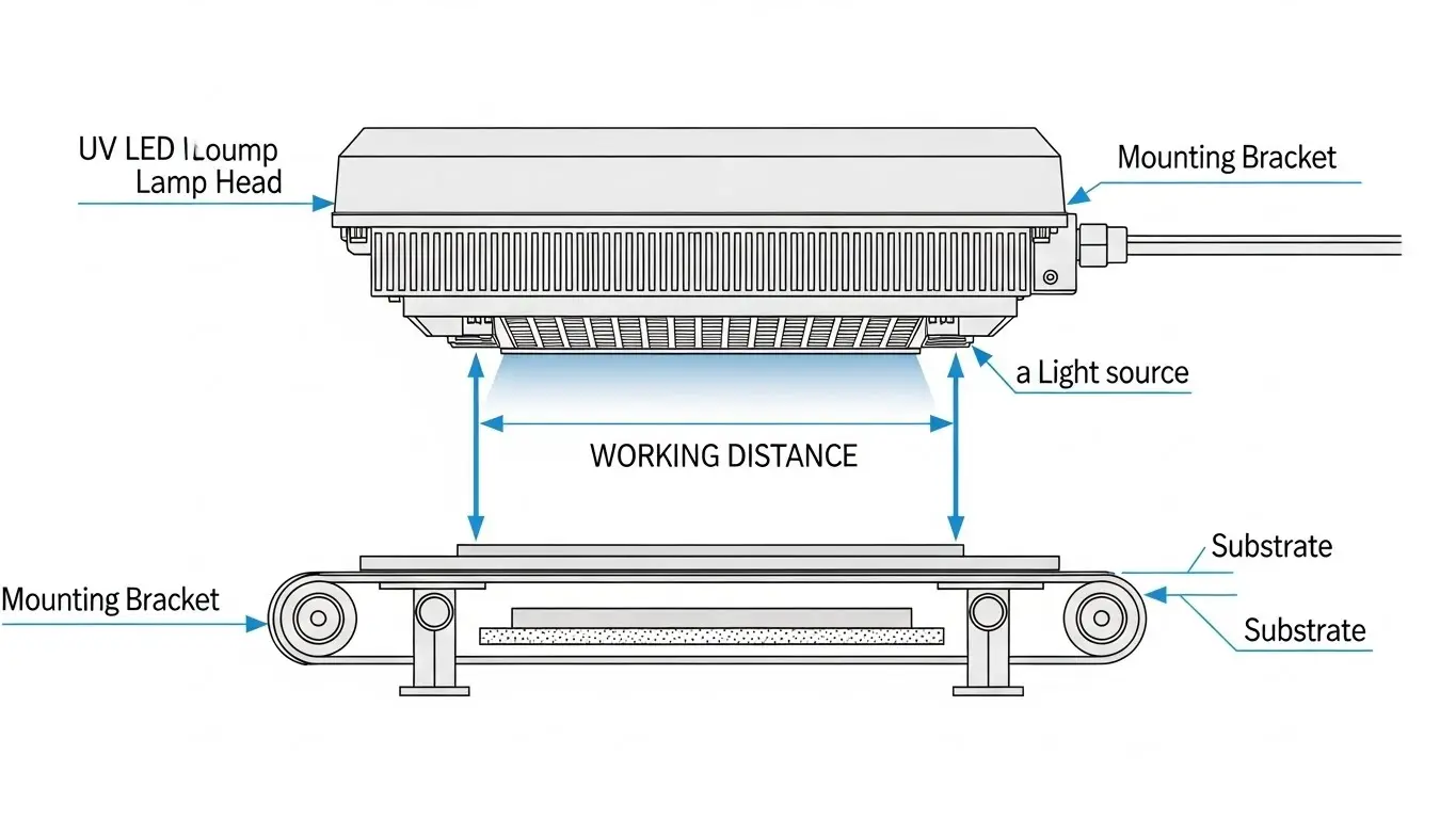
UV tape curing is important in the wafer processing during dicing and backgrinding. The adhesive qualities of the tape are weakened under controlled conditions when it is subjected to UV light. This will enable collecting single chips with ease without any damage. The process provides a clean release and stability of the wafer during critical operations.
- High Adaptability
Adaptability is one of the most notable features of the semiconductor tape curing systems that are used currently. UV-dicing tapes, treated, can be used not only with silicon substrates, but also with fine materials such as glass, ceramics, and compound semiconductors. This versatility implies that UV curing systems can be used across a broad range of applications in such industries as microelectronics, optoelectronics, and precision glass processing.
- Increased Process Productivity.
Faster speeds of response, coupled with the system-wide decreases in hold times, enable manufacturers to work with wafers more effectively. It reduces the adhesion of tapes on UV exposure, resulting in increased productivity with the same accuracy. Another method of minimizing downtime is the deployment of UV LED curing modules, which are instant on and have long service times.
Key Advantages
- Productivity Improvement
UV LEDs with cold light technology provide high efficiency by cutting down the adhesion of the tape in dicing and backgrinding. This not only makes handling of the wafer easier but also reduces the cycle time, which has an effect of improving overall yield.
- Cost-Effective and Green.
Recent UV curing systems do not contain mercury, and this means that they do not produce ozone. The systems are cost-effective and environmentally friendly with reduced energy consumption and long life of UV LED light sources, which are suitable in the current semiconductor fabs, and are sustainable.
- Easy to Operate
High-level curing systems have touchscreen controls with preset parameters. Curing intensity, timing, and wafer size settings can be easily modified by operators, making the process simple and friendly.
- Comprehensive Adaptability
The design of curing systems is such a way that it can be adapted to a variety of wafer diameters and types of tape, thus being used with different production requirements. They are reliable in curing performance, whether in an inline configuration in high-throughput manufacturing or a single bench configuration in an R&D project.
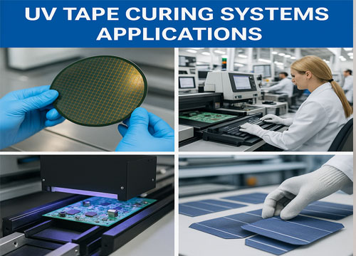
UV Tape Curing Systems Uses
The UV tape curing system is tailored to UV-sensitive adhesives, and hence, it would provide rapid and even curing. They are widely applied in:
- Micro-assembly - strong and stable adhesive bonds.
- Die bonding - enhancing bond integrity in semiconductor packaging.
- Wafer processing - This is to maintain stable adhesion in dicing and backgrinding.
- Glass processing/electronics assembly - allows low-heat curing (no risk) of adhesive.
These systems provide flawless curing with a reliable bond with low power drain, instant-on features, and fine-tuning capabilities that everyone would desire in a curing system; they satisfy high-tech industries.
Why Curing is Important in Semiconductor Manufacturing?
The semiconductor business requires microscopic efficiency. Any one failure of the adhesive can cost the company millions in production. Proper curing guarantees:
- Improvement in adhesion strength- steady bonding with stress.
- Integrity of material- avoidance of warpage and cracks.
- Great reliability curing - needed in the field of mission-critical electronics.
- Defect-free curing process - minimizing the expensive rework.
- Low temperature curing merit - securing delicate wafers.
Curing does not only involve hardening adhesives. It is concerning the performance of the electric part, thermal, and mechanical stability.
Machines and Tools of Tape Curing
Curing. The process entails high performance, and this demands precise equipment. Curing machines in use in semiconductor plants include:
- UV LED-cured modules - energy-saving, compact, and instant-on modules.
- Water-cooled UV curing systems - used when long duty cycles are required and the system should be stable.
- Automated curing systems - installed together with wafer handling instruments.
- Curing chambers of semiconductors - uniform curing at controlled temperatures.
- High-intensity UV LED treatment machines- used in high-throughput manufacturing lines.
Such systems offer regulated curing conditions, which are consistent and reproducible.
Perks of UV LED Semiconductor Tape Curing.
- Immediate action required no warm-up.
- Energy-saving curing solutions - reduced operating expenses.
- Cool curing - preserves frail wafers.
- Eco-friendly -RoHS and mercury-free.
- Bond formation with long duration of existence, which is required in high-reliability equipment.
- Small equipment size- easily fits in cleanrooms.
In semiconductor applications, UV LEDs are quickly becoming substitutes for old systems of curing.
Trends in Semiconductor Tape Curing Industry.
1. UV LED curing module shift-over of mercury lamps.
2. Automated curing solution- enhancing throughput and labor.
3. Combination with AI-based monitoring- ensuring the quality of curing.
4. The reduction of equipment to a smaller size- installation of modern cleanroom needs.
5. Sustainability - green semiconductor fab curing.
These trends indicate that curing solutions of semiconductor adhesives are changing to suit the future of electronics production.
Selection of the Appropriate Curing Equipment.
In choosing a curing system, consider into consideration:
- Tape type- dicing, backgrinding, or die attach.
- Volume of production - high-volume versus batch automated curing.
- Curing process: UV LED, thermal, or hybrid.
- System compatibility- compatibility with other tools in the system to handle the wafer.
- Cost efficiency -consumption of energy and maintenance.
Insight UV NDT on high-precision curing solutions.
Conclusion
Curing of semiconductor tapes is not just a technical process. It forms the foundation of the reliability of semiconductors. Curing helps in the bond perfection of adhesives, protection of wafers, and the survival of devices since wafer dicing all the way to packaging. Since the industry is shifting to UV LED semiconductor tape curing, the manufacturers are enjoying the benefit of more reliable, green, and faster processes. Energy efficiency, accuracy, and performance make UV curing the first of its type to become the choice of next-generation semiconductors. UVET is the source of information on UV LED curing modules and solutions.
Share on Social:


