
How UV LED for Electronics Supports Reliable Adhesive and Coating Curing
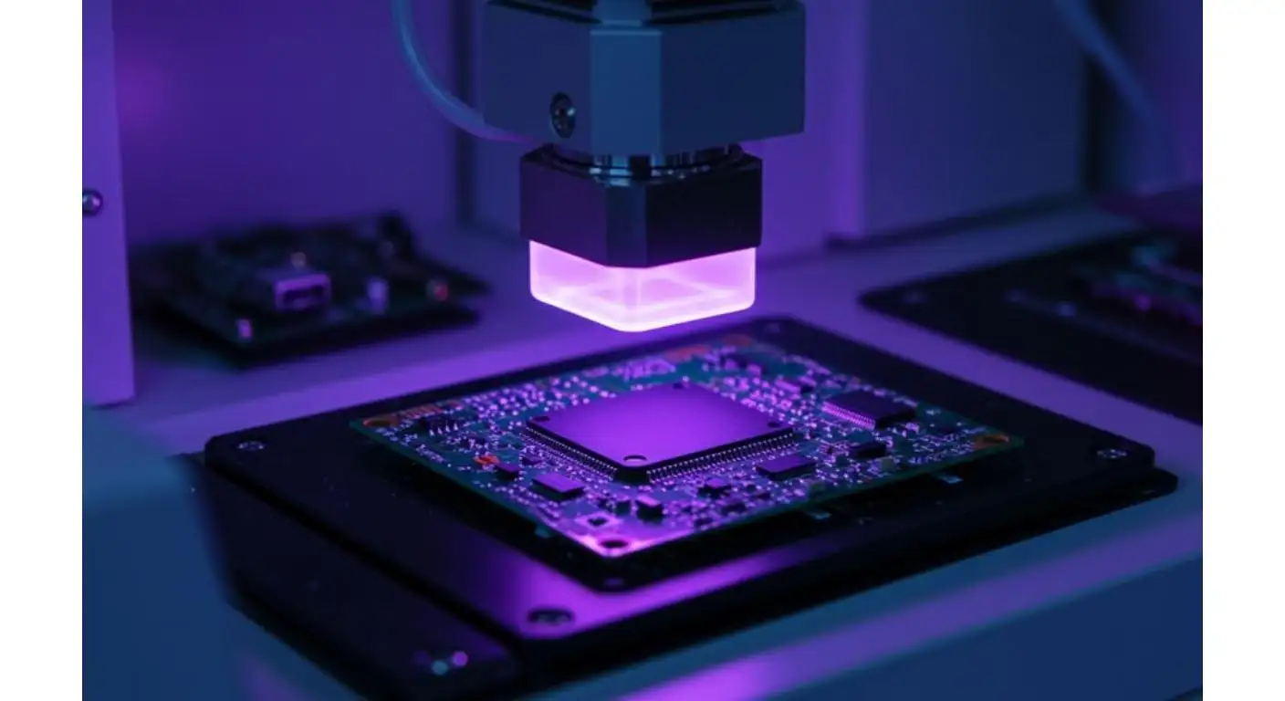
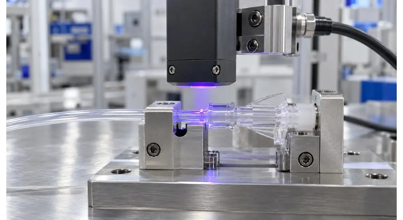
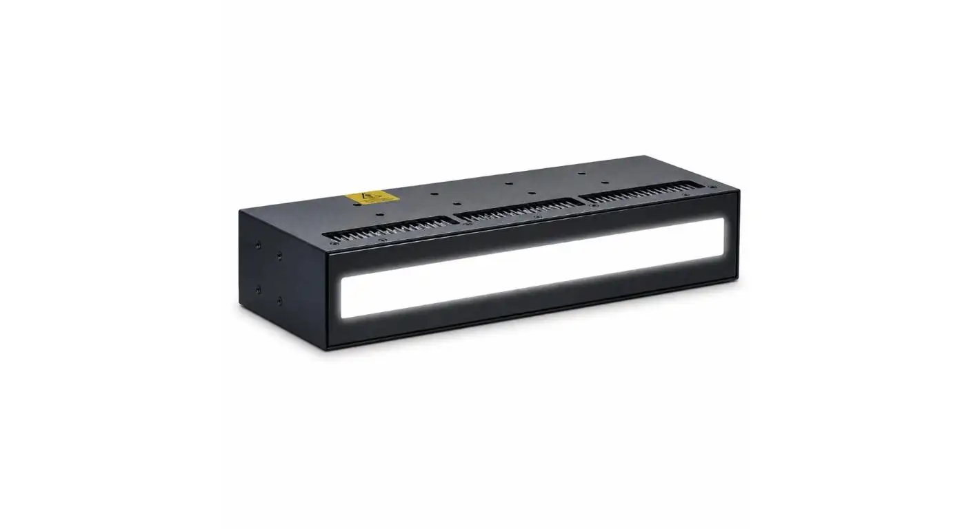
UV cured PCB coating can look like it has cured when it hasn't cured sufficiently next to tall components or the edges of the board. Light exposure can also be uneven in electronic adhesives and protective encapsulants, causing similar issues.
UV LED curing is consequently more than just a faster alternative to traditional curing methods, to the electronics manufacturer. The process should provide adequate exposure without impacting sensitive components or slowing down production.
The first step to successful implementation is to understand which materials need to be cured, how the light gets to them, and what the finished assembly will be judged on.
What are the Applications of UV LED in Electronics Industry?
UV LED curing is a process that employs specific UV wavelengths to promote the cure of compatible adhesives, coatings and encapsulants.
Applications in electronics are bonding of components, protective coatings, assembly of sensors, bonding and selected encapsulation processes of displays.
The amount of exposure required for each application is different.
Taking pictures of populated boards that require wide lighting is common with PCB coatings. Concentrated light is necessary for small adhesive bonds and careful attention to alignment and material properties is needed for optical assemblies.
The UVET UV LED for Electronics application guide is a guide to the technology that explains the range of applications in electronics including electronic components, circuit protection and precision assembly.
The key takeaway here is not all electronic materials are UV-curable. The material compatibility must be verified prior to choosing the curing equipment.
The importance of Exposure Uniformity on a PCB Assembly
Complex surfaces for UV exposure are found on populated circuit boards, in which the various components are of different heights.
Tall connectors, shielding structures and component housings: Light may not reach coatings under or next to tall connectors, shielding structures and component housings.
Even though the exposed surface may look good, these shadowed areas can contain uncured product.
The edges and corners of the boards may also be exposed to different levels of irradiation than the area in the middle.
When curing over a large area, engineers need to consider the actual UV distribution throughout the assembly and not just the maximum lamp intensity.
However, a broad irradiation field can be useful to enhance coverage provided that component geometry, fixture position and optical properties of the curing system are appropriate.
Select Curing Equipment that Corresponds to the Production Task
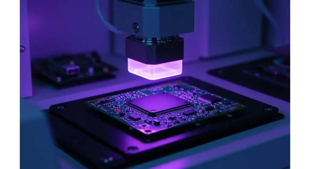
Spot, area and enclosed chamber curing setups are common amongst electronics manufacturers.
Appropriate for small adhesive joints to be locally exposed to cure. Larger area curing can be accomplished with area curing and enclosed chambers are available for prototype or batch processing in a controlled environment.
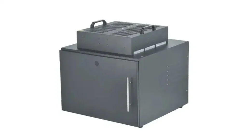
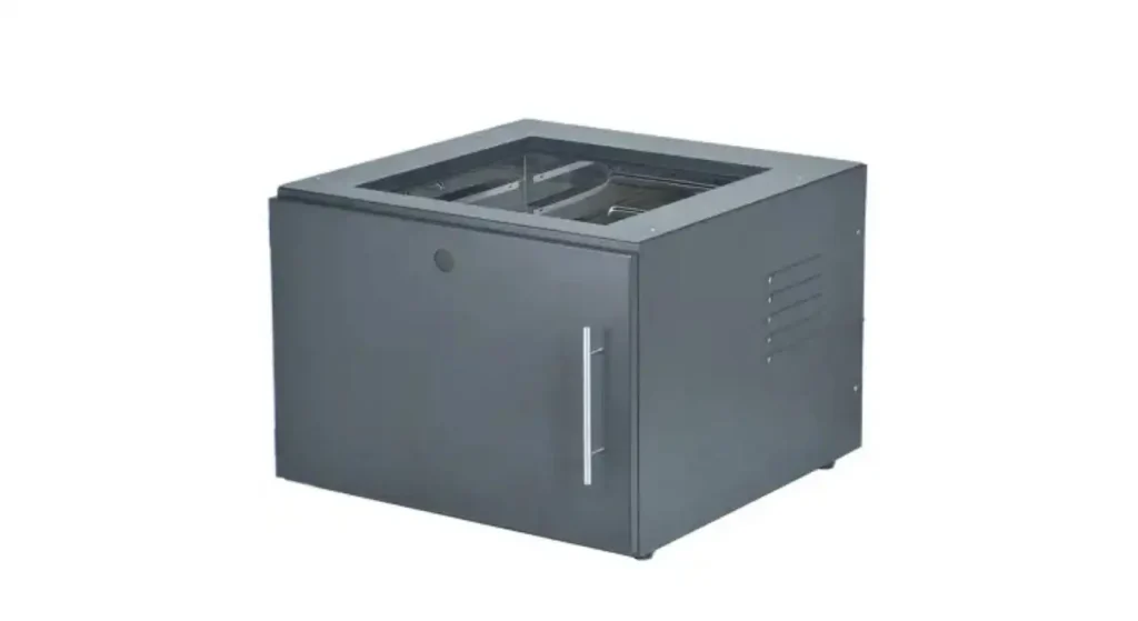
For laboratory testing and small batch production, UVET's UV LED Flood Curing Setup offers an enclosed working area with movable shelves.
The CS350B3 is 500 × 500 × 350 mm in size and can be configured in various different UV LED lamp setups.
It has a reflector design that helps to spread the irradiation in the chamber; the viewing window is used to view the curing process.
But real exposure uniformity should be determined using the employed light source and the arrangement of components.
Choose the Wavelength & Dose for Electronic Materials
UV-Curable adhesives and coatings contain photoinitiators which are capable of reacting to specific ranges of wavelengths.
Common UV LED options include 365 nm, 385 nm, 395 nm and 405 nm. The correct wavelength to use will depend on the formulation of the material and on manufacturer's recommendations.
The amount of UV dose is dependent on the intensity of UV that reaches the surface and the length of time the product is exposed.
For real-life electronics production, working distance, orientation of components and thickness of coating may affect the energy delivered.
With thicker encapsulants, surface curing may not ensure that the material is completely cured.
Process engineers should use real electronic assemblies to check the wavelength compatibility, dose and exposure time.
Use of POWDER PROTECT to protect sensitive components during the curing process.
Excessive temperature, mechanical stresses or dimensional changes are a problem for many electronic components.
Compared to traditional mercury UV lamps, UV LED systems emit less infrared radiation, which, however, does not mean there is no transfer of optical energy to the work piece and subsequent heat.
Monitoring of the curing temperature should be done with temperature-sensitive substrates, plastic housing and optical components.
Fixtures should also ensure assemblies without causing undue pressure on connectors or fragile parts.
Stable working distance, cooling and controlled exposure can help to maintain stable processing conditions.
This is especially important if a number of curing cycles is necessary in the product development phase.
| Electronics Task | Curing Arrangement | Main Selection Priority |
| Small adhesive joints | Spot UV LED | Precise exposure location |
| PCB conformal coatings | Flood UV LED | Wide-area uniformity |
| Multiple PCB samples | Enclosed UV chamber | Repeatable batch placement |
| Optical component bonding | Focused or area UV LED | Alignment and thermal control |
| Automated coating lines | Inline UV LED | Conveyor synchronization |
Create a Repeatable Batch Curing Process
For electronic prototypes, or for production involving mixed components, batch curing is available to provide flexibility.
But if multiple assemblies are placed within a single chamber this isn't necessarily the case and each part may be exposed to different amounts.
UV distribution can be affected by the number of boards, spacing of boards and the position of the shelf.
It is better to establish some standardized load configurations and prevent any stacking of the components in a manner that interferes with the light path.
The CS350B3 features a lamp interlock (door controlled) and an adjustable shelf. The UV lamp turns off when the door is opened, promoting safer handling of the UV lamp between curing cycles.
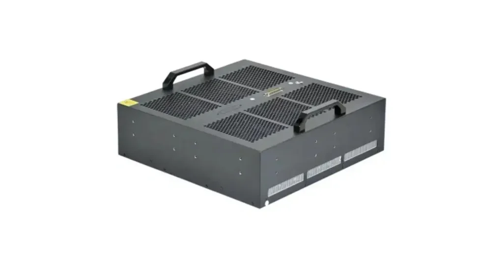
Meanwhile, if the required area to be processed is large, when selecting the equipment configuration, the manufacturer can also compare the UV LED Flood Curing System with other equipment configurations based on production volume and size of the processed components.
Using the IRC Methodology, this system verifies the performance of coating and bonding.
Visual inspection is not an adequate way to prove that an electronic adhesive or coating is in its required curing state.
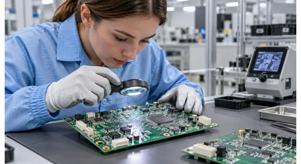
Checks that may be relevant to conformal coatings include adhesion, coverage, tack, coating thickness and material specific cure tests.
Mechanical strength test, alignment inspection or environmental reliability assessment is sometimes necessary for bonded parts.
Test samples must be made of real substrates, component heights, coating thickness and curing location.
In addition, engineers should assess the area in the most difficult to illuminate places, not only in the center, exposed areas.
Documented process limits enable a manufacturer to identify when material, equipment or loading arrangement changes are being made that may need further validation.
| Control Item | Verification Method | Acceptance Focus |
| UV distribution | Irradiance mapping | Meets validated exposure limits |
| Adhesive bonding | Mechanical strength test | Meets joint specification |
| Coating coverage | Visual or optical inspection | No unacceptable defects |
| Through-cure | Material-specific cure test | Adequate polymerization |
| Component temperature | Temperature measurement | Within approved limits |
| Batch repeatability | Repeated sample testing | Consistent results |
Take Maintenance and Process Documentation into account
The long-term curing consistency requires to maintain the light source and control the production process.
Optical contamination and aging of the equipment and operating conditions may result in changes to UV output.
Optical surface cleanliness, cooling performance and measured UV output are routine parameters which should be checked.
Production records should specify lamp configuration, exposure duration, loading configuration and material formulation approved.
Clear documentation of the processes minimizes the risk of using incorrect curing conditions with a new assembly for electronics manufacturers with multiple product variants.
Conclusion
UV LED for Electronics will offer a flexible method of curing compatible electronics adhesives, protective coatings & encapsulants.
The effectiveness of its use is not only related to the speed of cure, but also to whether it provides the proper wavelength and exposure to the complex electronic assemblies.
Manufacturers can compare the equipment geometry with the application, to control the batch loading and validate the finished material performance, to develop more consistent and reliable curing process.
FAQs
Q1. In the electronics manufacturing industry, what does UV LED do?
Cures compatible adhesives, coatings/encapsulants for protection in PCB, component bonding/electronic assembly. For each type of material and product geometry their respective applications vary.
Q2. Is it possible to use UV LED for the curing of PCB conformal coatings?
Yes, as long as the coating is designed to be UV cured. Shadowed areas may need another area of exposure or an approved secondary curing process.
Q3. Are sensitive electronic components safe to UV LED cure?
Can minimize thermal exposure relative to a number of the traditional curing procedures. But, compatibility of materials and temperature still need to be tested.
Q4. Spot or flood UV curing – what is the difference?
Spot curing can be used to shine light in small spots, and flood curing can shine light on larger surfaces. The method to be used is dependent on the size of the components and the coverage area.
Q5. What are the ways by which the manufacturer can check the quality of UV curing?
They should sample the amount of actual UV exposure and conduct appropriate adhesion, curing and reliability testing. The results must comply with the approved material and product specifications.
Share on Social:


