
Building a Reliable UV LED Process for Electronics Substrate Curing
It's not as easy as just putting a PCB under the brightest UV source to cure the electronics substrate. The process must produce the proper wavelength and UV energy without overheating the substrate or causing unneeded stress around sensitive components, or leaving material uncured in shaded areas.
The goal is to create a reproducible curing window for the process engineer that correlates the photosensitive material, the substrate configuration, the UV processing equipment and the rate of production. Therefore, the quality and consistency of the final electronic assembly should be used as an evaluation criterion for a well-designed industrial UV LED curing system, instead of the irradiance output.
Start with the Substrate and Photosensitive Material
The material specification should be the first point to consider when starting the curing process. These are some of the typical electronics applications of conformal coatings, component adhesives, encapsulants, solder mask coatings and protective coatings.
They can be used on rigid PCBs, flexible circuits, ceramic boards, glass, and metal-backed boards and thermally sensitive polymer films. UV and temperature are different for each substrate/material combination.
Find out the recommended wavelength, minimum UV dose, range of acceptable irradiance and maximum temperature from the material supplier. The thickness of the coating, color, contents and transparency should also be noted. Exposure techniques can vary depending on whether the material is thick or thin, dark or clear, or filled.
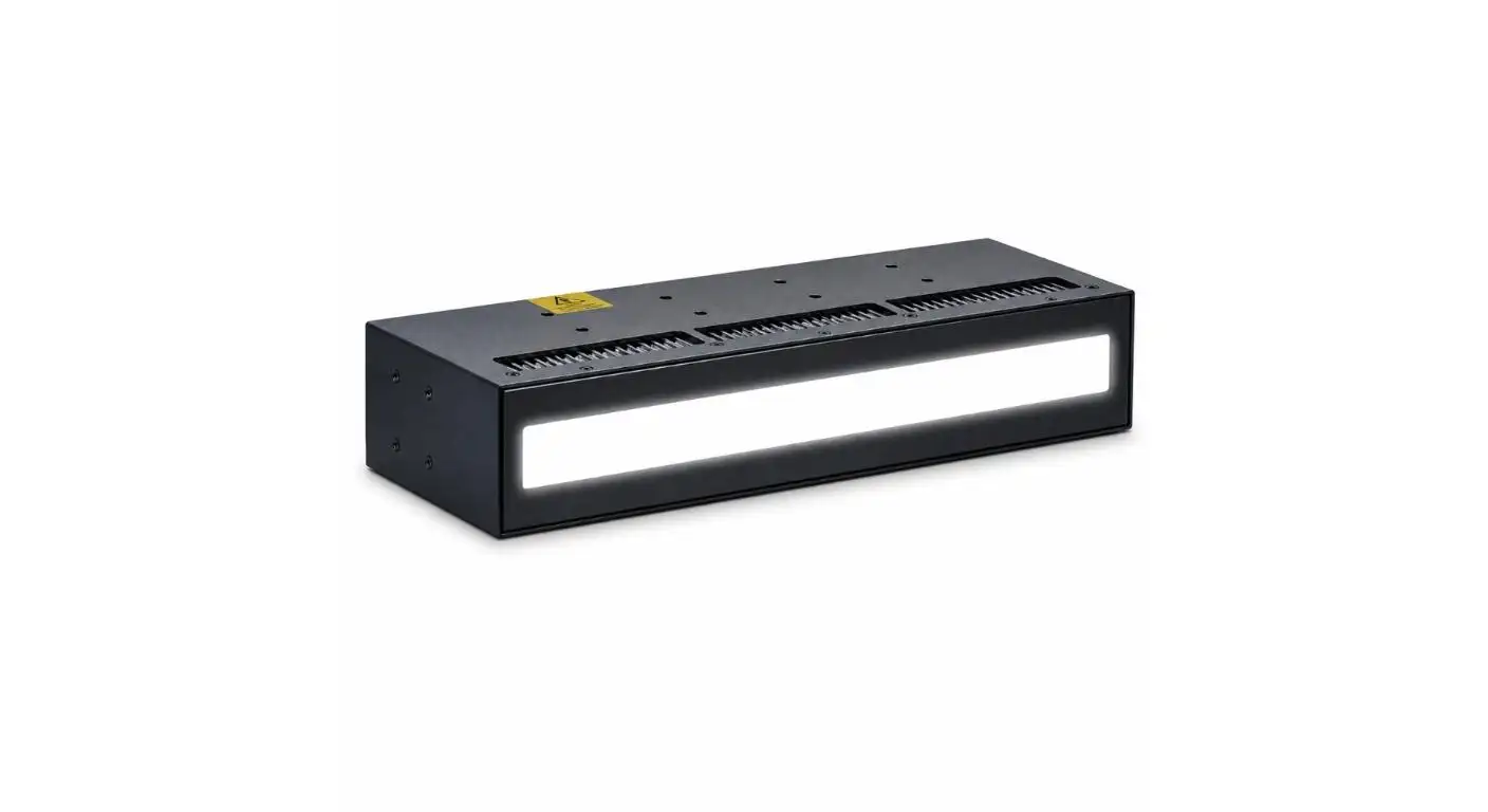
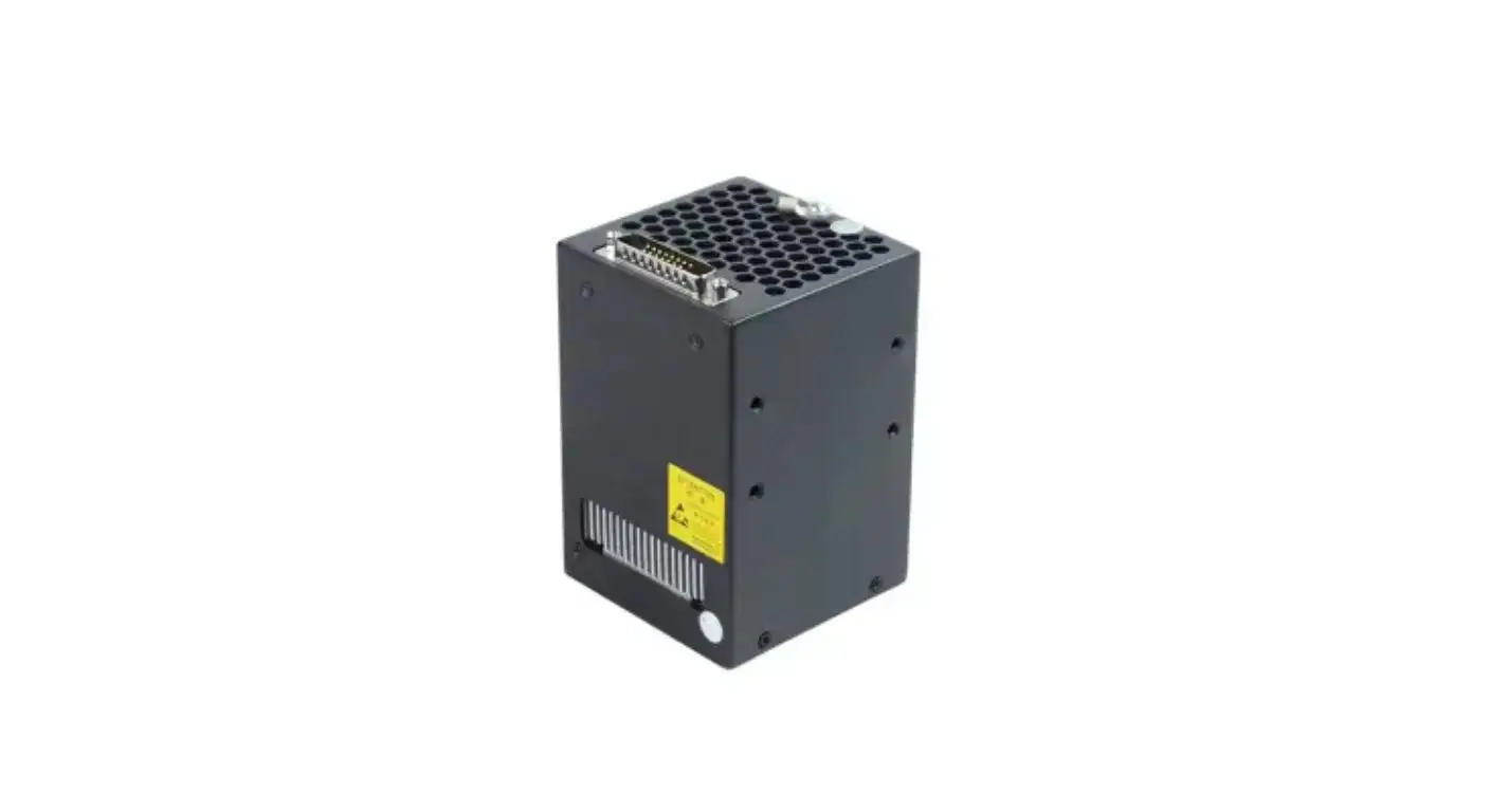
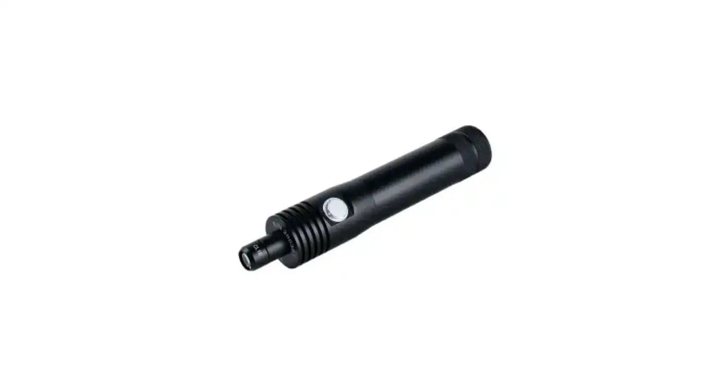
The company's UV LED electronics curing solutions show how controlled UV-exposure can be applied to PCB protection, display bonding and chip encapsulation and compact electronics module assembly.
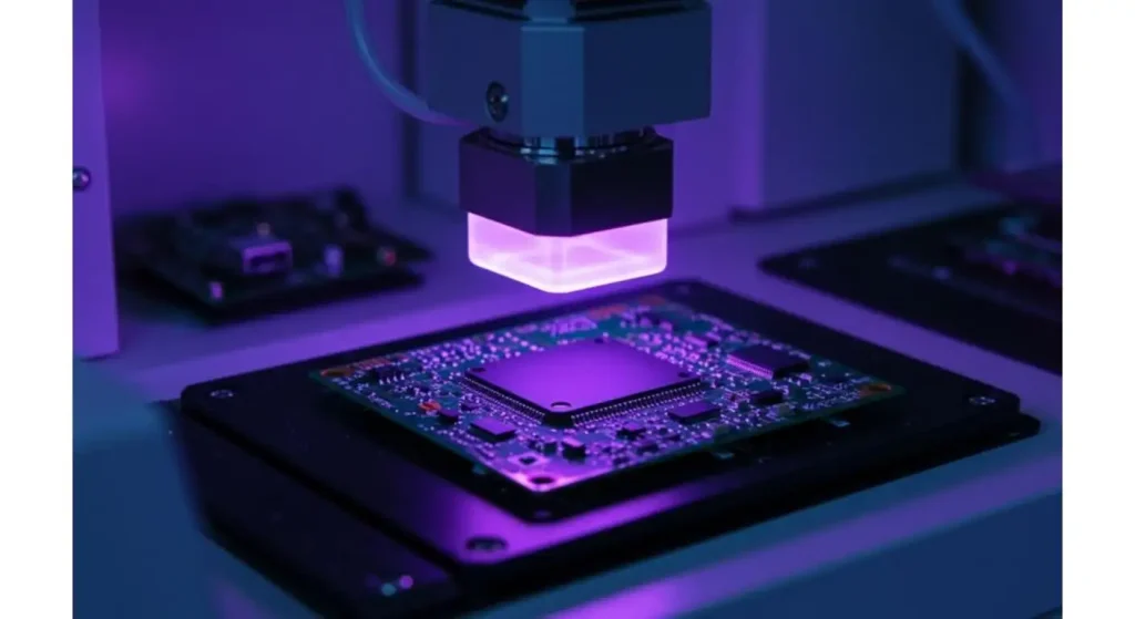
For each material, there is an optimal UV wavelength.
There is no substitute for good spectral compatibility for a high irradiance. The UV LED system's wavelength must overlap the photoinitiator's absorption range of the material.
In the industry, 365, 385, 395 or 405 nm are frequently employed. However the final selection should be based on the material specification and practical curing trials, rather than the general wavelength rule.
Before approving equipment, test the actual coating or adhesive on the substrate or surface to be coated. An apparently dry surface could have not fully cured material under it, particularly if the coating is thick and contains fillers and pigments.
| Process Variable | What to Confirm | Main Risk if Incorrect |
| Wavelength | Material absorption range | Limited photochemical reaction |
| Irradiance | UV power at the substrate | Insufficient activation or overheating |
| UV dose | Total energy received | Incomplete or excessive curing |
| Working distance | Actual production distance | Changed output and coverage |
| Exposure uniformity | Energy across the substrate | Uneven material performance |
Control Irradiance / Total UV Dose.
Irradiance is the amount of UV power applied to an area, dose is the amount of energy delivered during the curing cycle. Both impact on the end value.
It might not be the same effect if it is a long exposure at low irradiance compared to a short exposure at a high irradiance. The surface reaction is influenced by the level of peak intensity and the level of cure is influenced by the total amount of UV energy.
Use a compatible radiometer to measure the irradiance at the actual plane of the substrate. Output (working distance) as indicated at the lamp window may not be the only factor to consider, as energy to the substrate may be diminished due to working distance, optical components, and protective window.
The programmed exposure time should be noted along with the measured irradiance. This enables the engineer to compare curing trials and determine a range of controlled operation.
Test Uniformity of the Substrate within the Whole Substrate
Large PCB's, panelized assemblies and multiple substrates being processed in one cycle require uniform exposure. A good reading in the center does not necessarily mean a good reading on the edges.
Conduct multiple measurements of the various positions in the working area, such as the center, corners, and in critical areas where coatings or adhesive joints are present. Compare measurements against tests for post cure adhesion, hardness or other functional tests.
High components, connectors and fixtures can cause shadow effects. These areas may need to have the position of the substrate adjusted, or the angle of the substrate curing and/or sequence of the exposures changed. The goal is not just to light the board, but to provide enough UV energy to all of the functional curing areas.
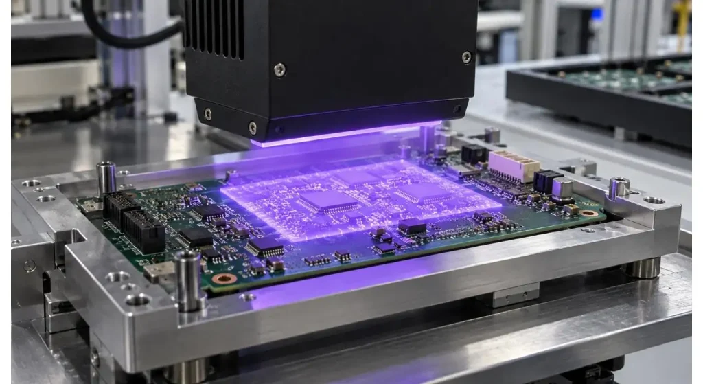
Do not allow Substrate Temperature to exceed Its Process Limit.
The amount of unwanted heat is generally less in UV LED curing than broad spectrum UV lamps, but substrate temperature needs to be monitored.
Locally high irradiance and short working distances and repeated cycles may increase temperatures. Flexible circuits can bend, polymer housings can warp and the components can be sensitive to temperature which can cause the parts to reach process limits.
Place temperature sensors for process trials at representative locations. Write down the highest temperature and the total time that it exceeded the chosen control limit. When the temperature of the substrate increases too rapidly, it can be cooled down by cooling airflow, adjusted working distance or divided exposure cycles.
Controllable exposure and instant switching are now available with modern LED UV curing systems, enabling the exposure cycle to be varied to meet the thermal tolerances of the electronic substrates.
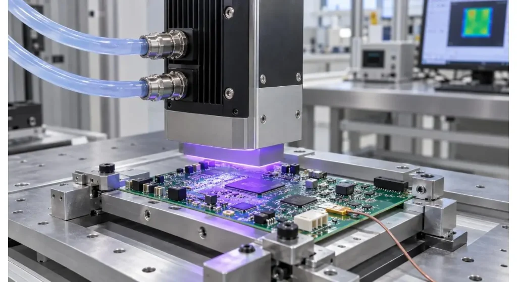
Select the right Industrial UV LED System for the Substrate.
The curing system should be chosen based on the parameters: Substrate size and position, component height and desired production speed.
Test the industrial UV LED curing system with real PCB, Flexible circuit or Electronic assembly. Check that its useful curing area, working distance, irradiance distribution and cooling performance are appropriate for the entire curing.
Fixture design is also crucial. For each exposure the substrate must be in the same position and orientation. If either the angle or the height of the material changes, it is possible that the UV energy reaching the material will change.
In the automated production, make sure that the exposure triggering, operation status, fault signals and cycle control can be integrated with existing equipment.
| Evaluation Item | What to Verify | Production Purpose |
| Curing area | Coverage of the substrate | Prevent untreated edge areas |
| Working distance | Distance used in production | Maintain repeatable irradiance |
| Fixture position | Stable substrate location | Reduce cycle variation |
| Cooling performance | Equipment and substrate temperature | Protect sensitive components |
| Control interface | Triggering, alarms and cycle signals | Support automated production |
| Output stability | Irradiance during repeated cycles | Maintain consistent curing |
Functional Tests to validate Cure Quality
A shiny or tacky surface is not an indication that the material is fully cured. The validation methods should be representative of the application of the cured material in the desired end-use electronic product.
Test requirements vary, depending on the use, and include surface tack, hardness, adhesion, solvent resistance, coating thickness, electrical insulation, bond strength, or optical clarity.
Set limits of acceptance prior to the trials. Note wavelength, irradiance, dose, working distance and exposure time for each sample and the temperature of the substrate and fixture position. This results in a traceable process window rather than on one good sample.
Check the repeatability before production release.
Laboratory sample provides only an indication of the possibility of curing. Production approval will need to show that the process is consistent over different substrates, material batches and runs.
Do a trial with the regular fixtures, material handling and production cycle times. Test samples at start, middle and end of run. Stability of the output should also be tested following frequent operation of the equipment.
UVET is a manufacturer of precision manufacturing UV LED curing equipment. Process engineers must validate the compatibility of controls, cooling and curing area of a system for the actual electronics production line.
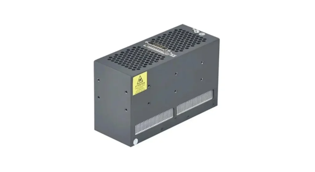
It is important to maintain the Validated Curing Window.
UV output, optical cleanliness, cooling performance and working distance should be included in preventive maintenance. When an optical window or fixture is contaminated, or a fixture is moved, the actual dose delivered at the same programmed exposure time will be reduced.
Set up a schedule to check the output of the radiometer and define an acceptable output range. A documented review and process revalidation shall be performed when changes are made to the coating, the adhesive, the substrate, the fixture, working distance or the UV equipment.
Conclusion
Wavelength compatibility, controlled irradiance, adequate UV dose, uniformity of exposure and substrate temperature are critical to reliable electronics substrate curing.
Specify material and substrates, measure UV energy at the real curing plane and perform functional tests. A production scale pilot run can then be used to determine if the industrial UV LED curing system offers the repeatability that is needed for electronic manufacturing.
FAQs
Q1. Which is the appropriate wavelength for curing of electronics substrates?
Common UV LED options include 365, 385, 395 and 405 nm. The appropriate wavelength will vary based on the particular photoinitiator in the material and will need to be verified via the material specification and curing trials.
Q2. Does a more intense UV mean it is better?
No; too much intensity will lead to increased surface reaction and higher temperatures for the substrate and will not guarantee complete depth curing. The three factors (irradiance, dose, and exposure time) must be considered as a group when assessing them.
Q3. How to check for uniformity in the curing process?
At the actual working distance, measure the irradiance at the center, corners and critical curing areas. Compare UV and adhesion, hardness or other functional test results.
Q4. Is it possible to cure material under large parts using UV?
Direct UV light may not be able to reach areas that are shaded by connectors or raised components. The position of the fixtures, curing angle/exposure sequence may require adjustment.
Q5. When it is time for revalidation of curing process?
Changes to material, coating thickness, substrate, fixture, working distance, exposure setting or UV curing equipment should be taken into consideration as the basis for revalidation.


